

 English
  Español
  Français
PCB in Electronics: Design Software, IPC Standards, Signal Integrity & ITAR Compliance
Content
- 1 What Is a PCB in Electronics
- 2 PCB Schematic Design Software: Tools and What They're Best For
- 3 IPC Standards for PCB Design: What They Cover and Why They Matter
- 4 Signal Integrity in PCB Design: Core Principles and Common Failure Modes
- 5 Fast Turnaround PCB Assembly: What Drives Lead Times and How to Compress Them
- 6 ITAR-Compliant PCB Manufacturing: Scope, Obligations, and What to Look For in a CM
What Is a PCB in Electronics
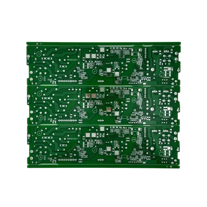
A printed circuit board (PCB) is the structural and electrical foundation of virtually every electronic device. It is a flat board — typically made from FR-4 glass-reinforced epoxy laminate — that mechanically supports and electrically interconnects electronic components through a network of conductive copper traces, pads, and vias etched or deposited onto its surface and inner layers. Without the PCB, modern electronics as we know them would be impossible: it replaces the point-to-point wiring of early electronics with a compact, repeatable, and manufacturable structure.
A PCB serves three fundamental roles simultaneously. First, it provides the physical platform on which components — resistors, capacitors, integrated circuits, connectors, and hundreds of other parts — are mounted and soldered. Second, it creates the electrical pathways that allow signals and power to travel between those components with precision. Third, it performs this routing in a format that can be mass-produced with consistent quality at scale, from consumer electronics shipped in the billions to aerospace hardware produced in single units.
PCBs are categorized by layer count and construction. Single-layer boards carry traces on one side and are common in low-cost consumer products. Double-sided boards use both surfaces. Multilayer PCBs — typically 4, 6, 8, or more layers — are standard in any application involving dense component placement, controlled impedance, power integrity planes, or high-speed digital signals. High-density interconnect (HDI) boards take this further, using microvias and fine-pitch features to pack more circuitry into a smaller footprint, as seen in smartphones and wearables.
Beyond the standard rigid FR-4 construction, flexible PCBs (flex circuits) use polyimide substrates to allow bending and folding into three-dimensional shapes — essential in medical devices, aerospace wiring, and compact consumer electronics. Rigid-flex boards combine both technologies in a single assembly, eliminating connectors and reducing weight and failure points in demanding environments.
PCB Schematic Design Software: Tools and What They're Best For
Schematic capture is the starting point of PCB design — it defines the logical connections between components before any physical layout begins. The schematic is then used to generate a netlist that drives the PCB layout tool. Choosing the right EDA (electronic design automation) software affects not only the design experience but also DFM (design for manufacturability) outcomes, collaboration workflows, and compliance documentation.
The major platforms in professional PCB design are:
- Altium Designer: The dominant choice in professional hardware engineering. Known for its unified schematic-to-layout environment, strong library management, and comprehensive design rule checks (DRCs). The ActiveBOM and MCAD co-design features are particularly valued in product development workflows. Licensing costs are high, but the depth of functionality justifies it for full-time PCB engineers.
- KiCad: The leading open-source EDA platform. Version 7 and beyond have closed much of the gap with commercial tools, offering a capable schematic editor, 3D visualization, differential pair routing, and a growing community library. Widely used in startups, open-hardware projects, and academic settings.
- Cadence OrCAD / Allegro: OrCAD is widely used for schematic capture in engineering firms, while Allegro is the high-end layout tool preferred for complex multilayer boards and high-speed signal integrity work. Strong SPICE simulation integration makes OrCAD a go-to for analog and mixed-signal design teams.
- Mentor PADS / Xpedition: Common in automotive and industrial electronics. PADS is a mid-range option for smaller teams; Xpedition is enterprise-grade with strong constraint-driven layout for high-speed and RF applications.
- EasyEDA / Fusion 360 Electronics: Cloud-based platforms suited to prototyping, hobbyist work, and teams needing rapid design-to-fabrication workflows. EasyEDA is tightly integrated with JLCPCB's assembly service, enabling one-click fabrication quoting directly from the design environment.
Regardless of tool choice, the schematic must include complete and accurate component values, reference designators, and pin assignments — errors in the schematic propagate directly into the manufactured board. Most professional workflows enforce a formal schematic review against the design specification before layout begins.
IPC Standards for PCB Design: What They Cover and Why They Matter
IPC (formerly the Institute for Printed Circuits, now simply IPC — Association Connecting Electronics Industries) publishes the globally accepted standards that govern PCB design, fabrication, assembly, and inspection. Compliance with IPC standards is not optional in most professional and regulated industries — it is contractually required by OEMs, defense primes, and medical device manufacturers, and is frequently audited.
| IPC Standard | Scope | Applies To |
|---|---|---|
| IPC-2221 | Generic PCB design standard — trace width, spacing, hole sizes, thermal relief | All PCB designers |
| IPC-2222 / 2223 | Rigid and flexible board sectional design requirements | Rigid and flex PCB layout engineers |
| IPC-A-600 | Acceptability of printed boards — visual and microsection inspection criteria | Fabricators and incoming inspection teams |
| IPC-A-610 | Acceptability of electronic assemblies — solder joint quality, component placement | PCBA assemblers and quality inspectors |
| IPC-7711/21 | Rework, modification, and repair of electronic assemblies | Repair technicians and MRO operations |
| IPC J-STD-001 | Requirements for soldering electrical and electronic assemblies | SMT and through-hole assembly operations |
IPC-A-610 and J-STD-001 define three product classes — Class 1 (general electronics), Class 2 (dedicated service electronics), and Class 3 (high-reliability, including military and medical). Class 3 imposes the most stringent solder joint, cleanliness, and workmanship requirements, and demands certified IPC operators and inspectors (CIS/CIT) on the production floor. Specifying the wrong class — or failing to specify one at all — is a common source of quality disputes between buyers and contract manufacturers.
Signal Integrity in PCB Design: Core Principles and Common Failure Modes
Signal integrity (SI) refers to the quality of an electrical signal as it travels through the PCB — specifically, whether it arrives at its destination with sufficient amplitude, timing accuracy, and shape to be correctly interpreted by the receiving device. As clock speeds and data rates have climbed into the gigahertz range, signal integrity has moved from a niche concern to a mainstream design discipline. A board that passes DRC and looks correct in layout can still fail functional testing due to SI problems invisible to the eye.
The most common signal integrity issues and their design-level mitigations include:
- Impedance discontinuities: Any change in trace geometry — width transitions, vias, connectors, stubs — creates a local impedance change that causes partial signal reflection. Controlled impedance routing (typically 50Ω for single-ended, 100Ω differential) and via stub mitigation (back-drilling or blind vias) are standard countermeasures.
- Crosstalk: Electromagnetic coupling between adjacent traces induces noise on quiet lines. Increasing trace spacing (3W rule: space equal to 3× trace width edge-to-edge), using ground guard traces, and routing high-speed signals on inner layers between ground planes all reduce crosstalk.
- Return path discontinuities: High-frequency return currents follow the path of least inductance — directly beneath their forward-current trace on the reference plane. Cuts, slots, or plane changes that interrupt this return path force the current to detour, creating a loop antenna that radiates EMI and injects noise into other circuits.
- Skew in differential pairs: Differential signaling (PCIe, USB, HDMI, DDR, LVDS) depends on both conductors being electrically matched in length. Length mismatch introduces skew — a timing offset between the P and N signals — that degrades eye diagram margin and increases bit error rate. Most EDA tools enforce differential pair length matching via interactive routing constraints.
- Power delivery network (PDN) noise: Insufficient bypass capacitance or poorly placed decoupling capacitors allow voltage fluctuations on power rails when ICs switch. This manifests as ground bounce, supply noise, and increased jitter in clock signals. PDN analysis tools model impedance vs. frequency to guide capacitor selection and placement.
Pre-layout simulation (using IBIS models and transmission line calculators) and post-layout extraction (using 3D electromagnetic field solvers such as Ansys HFSS or Cadence Sigrity) are standard practices on high-speed boards. At data rates above 10 Gbps, SI analysis is not a post-design verification step — it is an input to the stackup and routing strategy from day one.
Fast Turnaround PCB Assembly: What Drives Lead Times and How to Compress Them
Fast-turnaround PCB assembly — delivering functional boards in 24 hours to 5 days rather than the standard 10–15 business days — has become a competitive differentiator among contract manufacturers (CMs) serving prototyping, NPI, and urgent production requirements. Understanding what actually drives assembly lead times allows buyers to make smarter choices rather than simply paying premium rates for service that may not deliver faster results.
The main contributors to assembly lead time are:
- Bare board fabrication: Standard FR-4 multilayer boards (up to 8 layers) can be fabricated in 24–48 hours by quick-turn fabricators. Advanced constructions — HDI, Rogers laminates, buried vias, controlled impedance — add 1–5 days depending on complexity.
- Component availability: This is typically the longest lead-time variable. A design relying on single-source or allocated components can stall assembly for weeks regardless of CM capabilities. Building a BOM around parts stocked by major distributors (Digi-Key, Mouser, Arrow) dramatically improves turnaround predictability.
- Programming and test: In-circuit test (ICT), functional test, or firmware programming adds time that is largely fixed regardless of batch size. On very small prototype runs, test setup time can exceed assembly time.
- Documentation quality: Incomplete or ambiguous Gerber files, missing centroid data, or an unresolved BOM drive engineering queries that add days to every fast-turn job. Submitting clean, complete packages — including assembly drawings, approved vendor lists, and a resolved BOM — is the single most controllable lead-time reduction lever available to the buyer.
CMs offering genuine 24-hour assembly typically maintain a consignment inventory of common passives (0402/0603 resistors and capacitors in E24/E96 series), run double-shift SMT lines, and have an engineering team on-call to resolve DFM queries without business-hours bottlenecks. For production quantities, true fast-turn capability requires pre-positioning material and scheduling machine time in advance — ad-hoc rush jobs at production scale are rarely reliable.
ITAR-Compliant PCB Manufacturing: Scope, Obligations, and What to Look For in a CM
The International Traffic in Arms Regulations (ITAR) is a U.S. regulatory framework administered by the Directorate of Defense Trade Controls (DDTC) under the State Department. It controls the export and import of defense articles, defense services, and related technical data listed in the United States Munitions List (USML). PCBs designed or used in military, satellite, weapons, or certain dual-use systems are frequently ITAR-controlled, and any CM that fabricates, assembles, or even handles technical data for these boards must comply with ITAR requirements.
ITAR compliance for a PCB contract manufacturer involves several specific obligations:
- Registration with DDTC: Any U.S. company that manufactures, exports, or brokers ITAR-controlled defense articles must register with the DDTC. This registration must be current and renewed annually.
- Foreign national access controls: ITAR restricts access to controlled technical data — including PCB Gerber files, design documentation, and assembly drawings — to U.S. persons (citizens, lawful permanent residents, or those granted protected status). CMs must have documented procedures to prevent foreign nationals from accessing ITAR-controlled data without an export license or applicable exemption.
- Physical segregation: ITAR-controlled work areas, storage systems, and data servers must be physically or logically segregated from non-ITAR work to prevent inadvertent disclosure.
- Subcontractor flow-down: If an ITAR-registered CM outsources any portion of the work — bare board fab, conformal coating, testing — to a subcontractor, ITAR obligations flow down. The prime CM is responsible for ensuring subcontractors are also ITAR-registered and compliant.
- Record keeping: ITAR requires manufacturers to maintain records of all transactions involving ITAR-controlled articles for a minimum of five years.
When qualifying an ITAR-compliant PCB CM, buyers should request a copy of the supplier's current DDTC registration, review their Technology Control Plan (TCP), and verify that their facility security posture — including IT systems, visitor access, and employee screening — matches the classification level of the work being placed. Penalties for ITAR violations are severe: civil fines up to $1 million per violation and criminal penalties including debarment from future government contracting. Vetting a CM's ITAR posture before program award, not after first article inspection, is the industry-standard approach.


 LET'S CREATE THE FUTURE TOGETHER

Contact Us Anytime
Copyright © Anhui Hongxin Electronic Technology Co., Ltd. All Rights
Reserved.
privacy
Wholesale Printed Circuit Board Suppliers, Manufacturers
![]()
